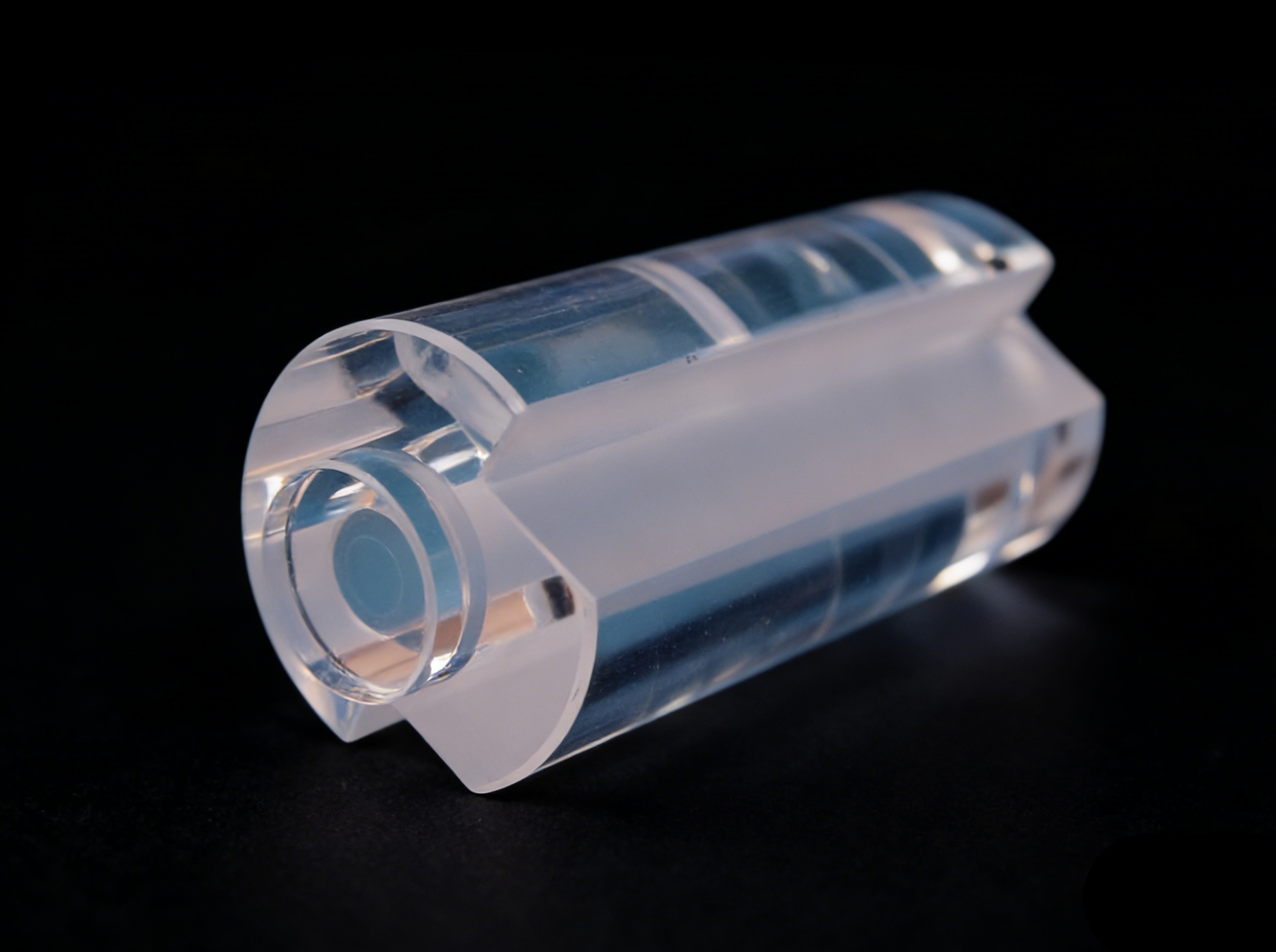
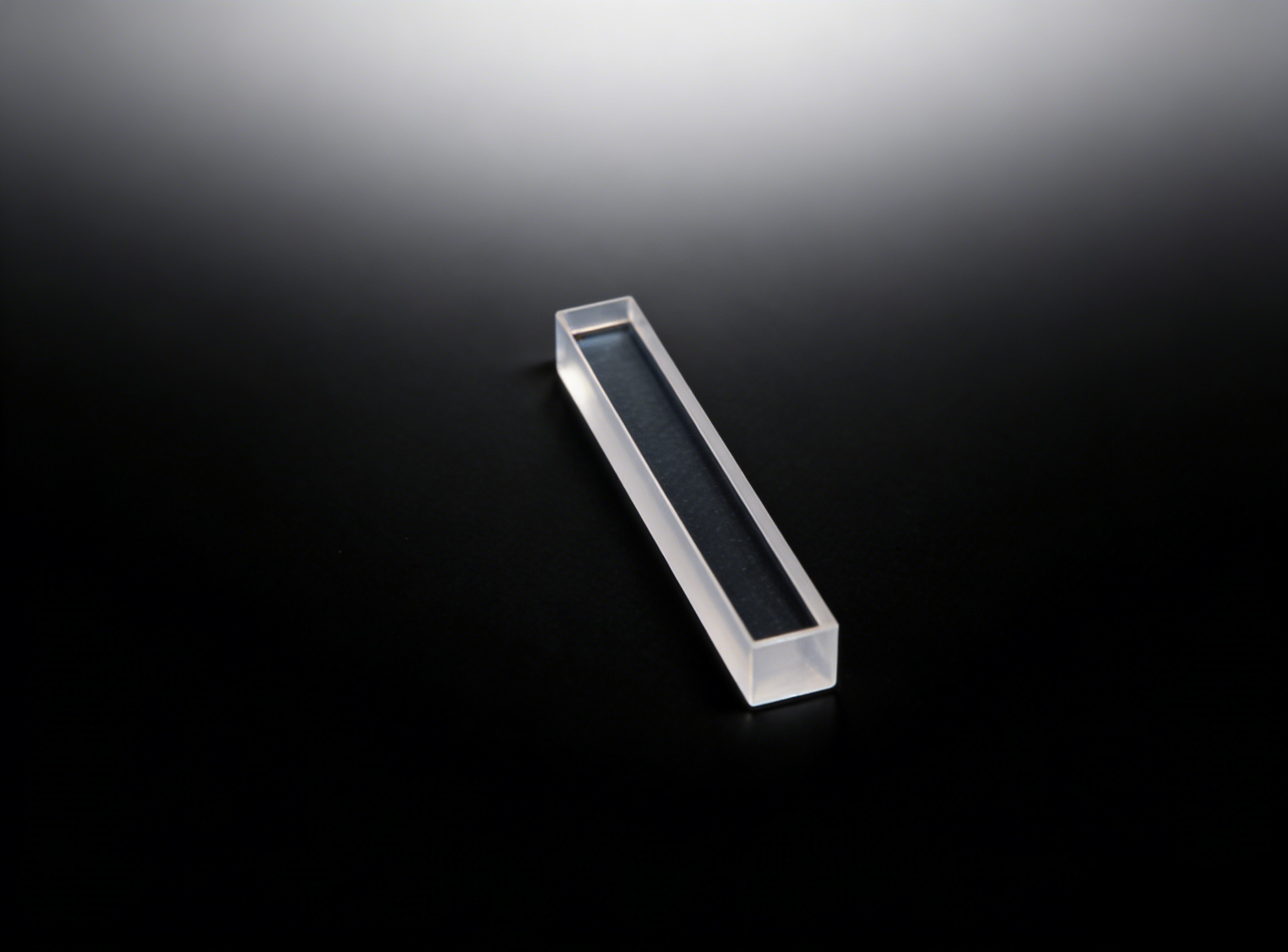
Super smooth long strip mirror
Our ultra-smooth long strip mirror is a high-end precision optical component specifically designed for lithography machines and wafer inspection fields. It achieves ultimate optical performance through ultra-fine polishing process, with strict control over size specifications and proportions. It meets the demanding application requirements of high-end semiconductor manufacturing inspection equipment and provides high-precision and low-loss optical support for lithography and wafer inspection systems.
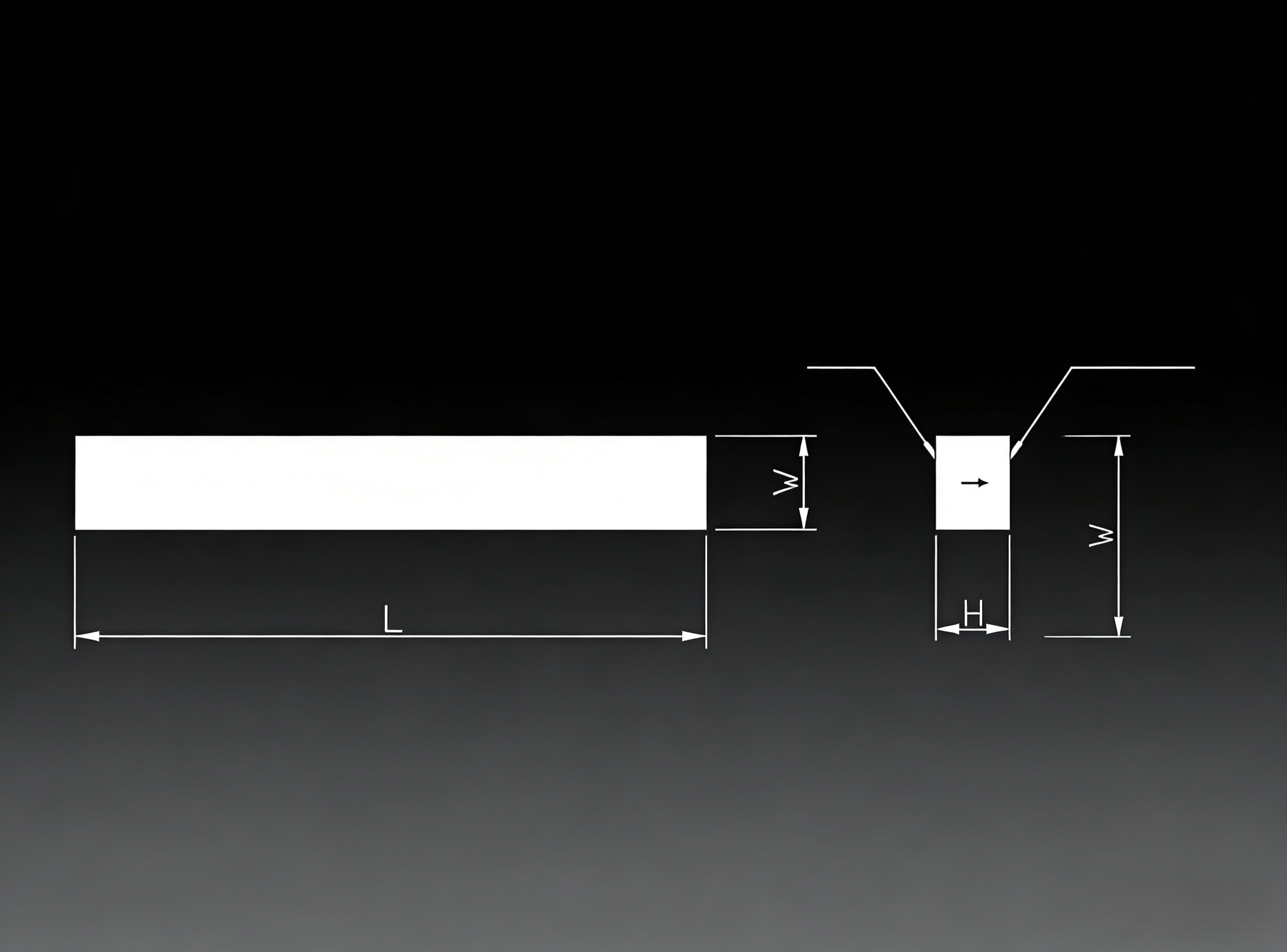
Core product parameters
Screening metrics | Specific parameters |
External dimensions and tolerances | L=3mm to 150mm, W=3mm to 150mm; H=3mm to 50mm Tolerance ±0.1mm; L:W > 10:1; L:H > 8:1 |
Surface shape accuracy | λ/5 @632.8nm |
Surface defects | 10-5 |
Surface roughness | Ra0.15nm (Zygo profilometer, 173*173um test area, 50x lens full frequency measurement) |
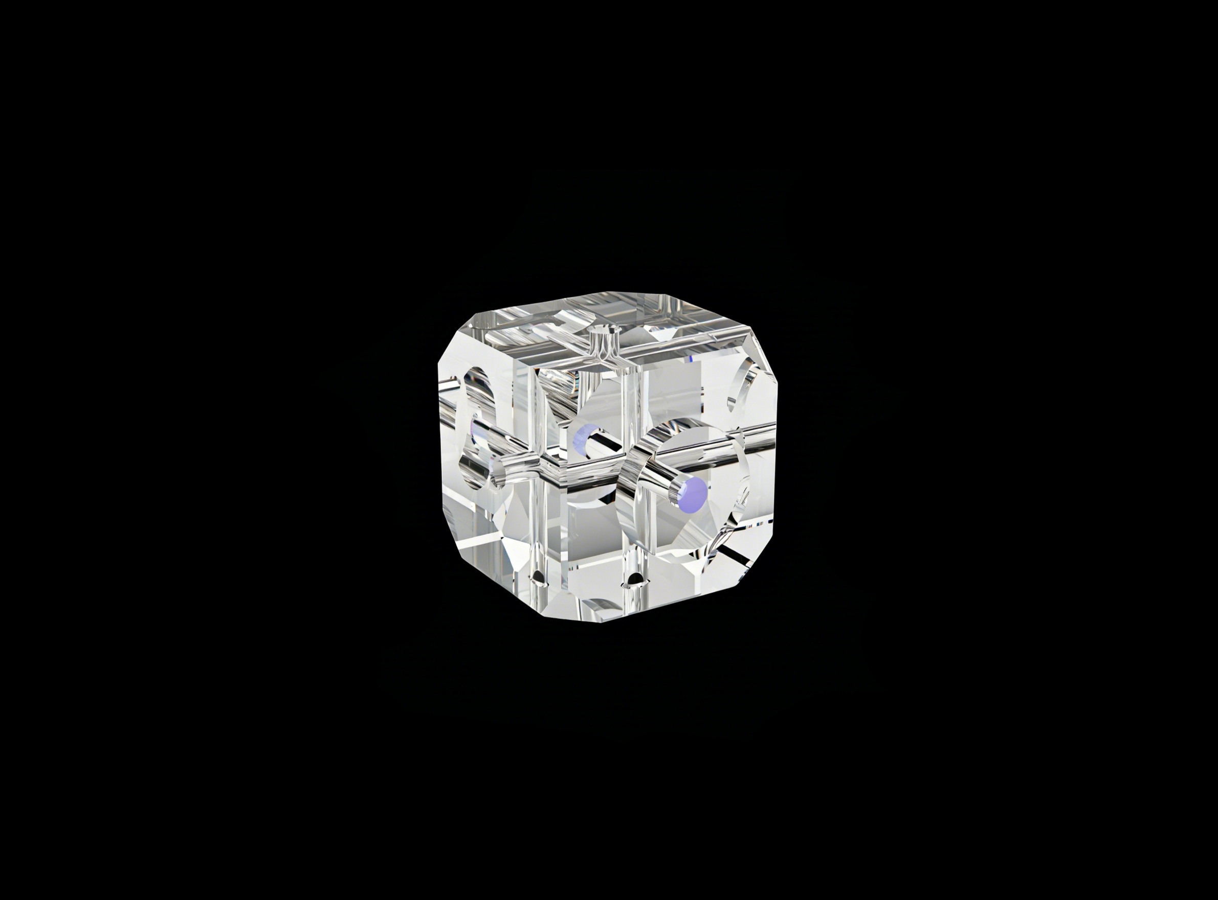
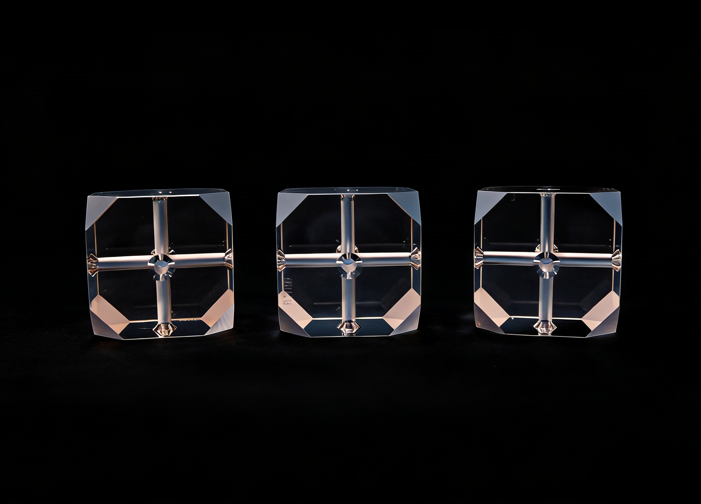
Substrate material | Fused quartz glass, sapphire |
Product Core Advantages
Exclusive field fit:
Tailored for high-end applications such as lithography machines and wafer inspection, size ratios strictly follow L:W > 10:1, L:H > 8:1 standards, perfectly matching the optical system assembly requirements of the equipment.
Superior optical accuracy:
Surface shape accuracy up to λ/[email protected], surface roughness as low as Ra0.15nm, significantly reduces light transmission loss and ensures the accuracy of optical signals in the lithography and inspection process.
Strict dimensional control:
Full dimensional tolerance strictly controlled ±0.1mm, high dimensional accuracy, direct assembly without secondary processing, improving customer production efficiency and reducing matching costs.
High specification surface quality:
Surface defects up to 10-5 industry high standards, no obvious defects, effectively avoiding light scattering and refraction deviations, meeting the ultimate optical requirements of semiconductor high-end processes.
High-end substrate selection:
Selected fused quartz glass and sapphire as substrates, with high-temperature resistance, laser damage resistance and structural stability, can operate stably for a long time in complex conditions of lithography machines.
Core application areas
Core applications in high-end semiconductor manufacturing and inspection fields such as lithography machines and wafer inspection are key optical components in semiconductor lithography systems and wafer inspection equipment, providing core optical support for the stable and efficient operation of high-end semiconductor manufacturing processes