2025 World Photonics Congress (Beijing) Exhibition Preview
Exhibition Preview of the 2025 World Photonics Congress (Beijing)
 Exhibition Preview")
 Exhibition Preview")
I. Basic Information of the Exhibition
The full name of the exhibition:
The 6th World Photonics Congress & The 14th International Conference on Applied Optics and Photonics Technology & The 16th China Optoelectronics Industry Expo (WPC 2025/AOPC 2025/PHOTONICS CHINA 2025
Organizers:
Chinese Society of Optics and Optoelectronics, International Society for Optics and Photonics (SPIE)
Event Dates:
June 24th - June 27th, 2025 (June 24th for academic conference, June 25th - 27th for exhibition and display)
Venue:
National Convention Center, Beijing (No. 7, Tianchen East Road, Chaoyang District, Beijing)
Exhibition positioning:
A top domestic and internationally renowned all-industry-chain event in the photonics field, integrating academic exchanges, achievement displays, business connections, and the integration of industry, academia, and research, leading the technological innovation and high-quality development of the optoelectronic industry.
II. Exhibition Scale and Zone Planning
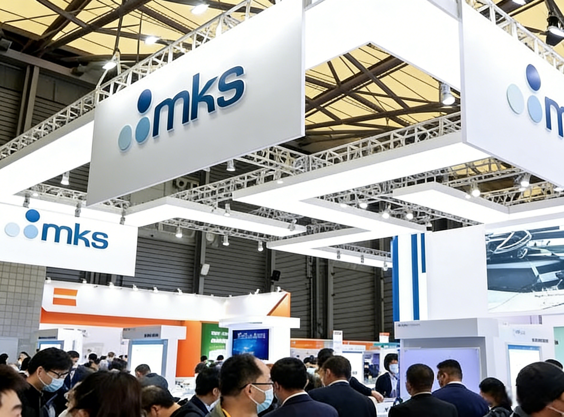
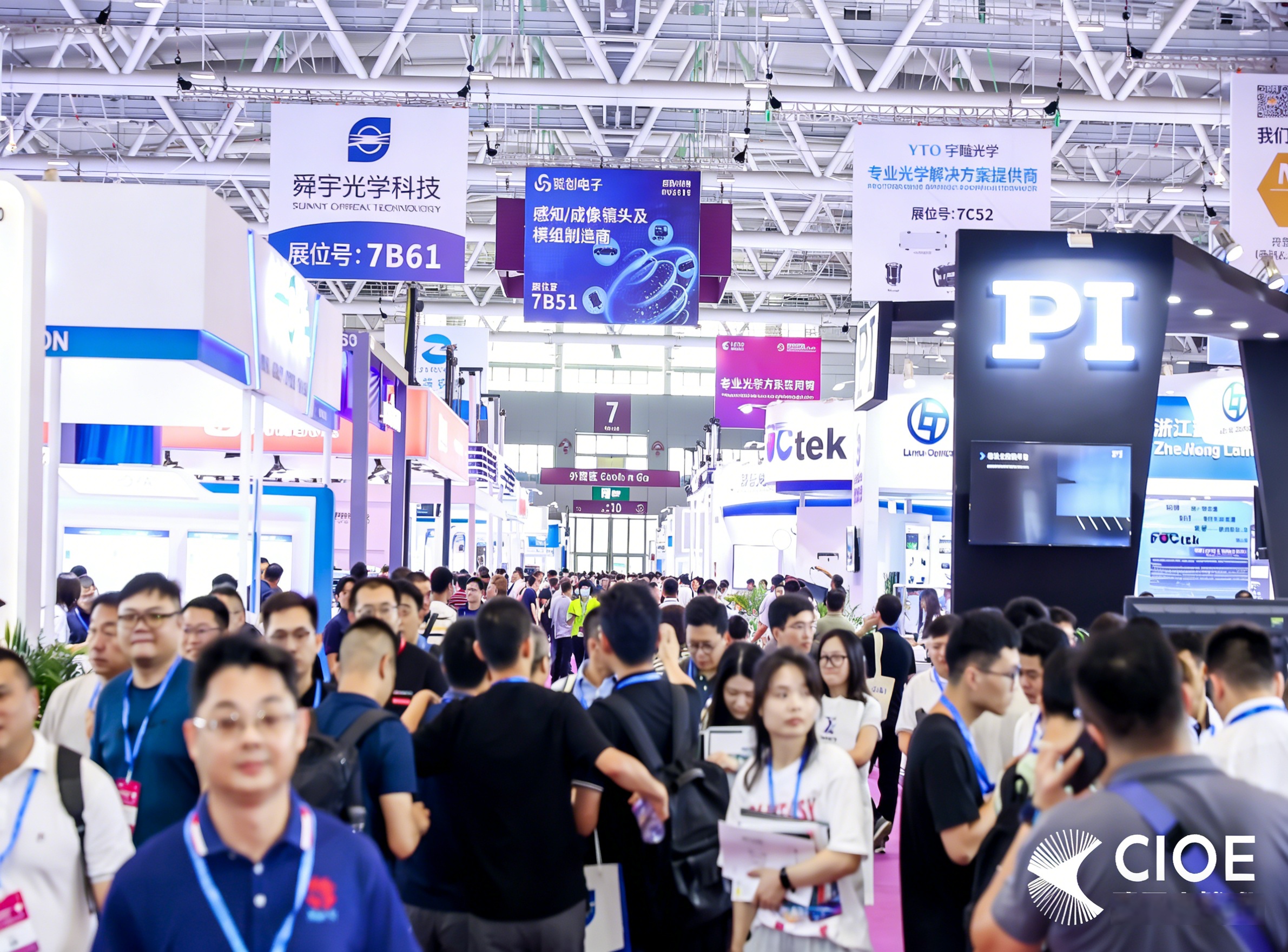
The exhibition area of this year's conference exceeds 30,000 square meters, gathering over 600 leading exhibitors from home and abroad and more than 3,000 global industry elites. Focusing on the core fields of optoelectronics, it sets up eight distinctive exhibition zones, covering the entire industrial chain of products and technologies.
Laser Intelligent Manufacturing Exhibition Area:
Industrial lasers, laser processing equipment, laser precision detection, laser 3D printing and supporting solutions.
Infrared Technology and Application Zone:
Infrared detectors, infrared thermal imagers, infrared optical components, security/medical/industrial infrared application systems
Precision Optics and Optical Manufacturing Zone:
Optical components, optical lenses, optical coatings, optical processing and inspection equipment, optical design software
Optical Communication and Optical Sensing Exhibition Area:
Optical modules, optical fibers and cables, optical transmission equipment, photoelectric sensors, optical application solutions for the Internet of Things
Micro-nano Optics and Quantum Optics Exhibition Area:
Micro-nano photonic devices, quantum light sources, quantum sensing, nano-optical materials and manufacturing technologies
Optoelectronic Detection and Imaging Exhibition Area:
Machine Vision, High-Speed Imaging, Spectral Detection, Computational Imaging Equipment and Systems
Optoelectronic Chip and Integrated Exhibition Area:
Optoelectronic chips, integrated optical devices, silicon photonic modules, semiconductor optoelectronic materials
Frontier Optoelectronic Achievements Exhibition Area:
Scientific research achievements from universities and research institutes, new products from specialized, refined, distinctive and innovative enterprises, and demonstration projects of new optoelectronic productivity.
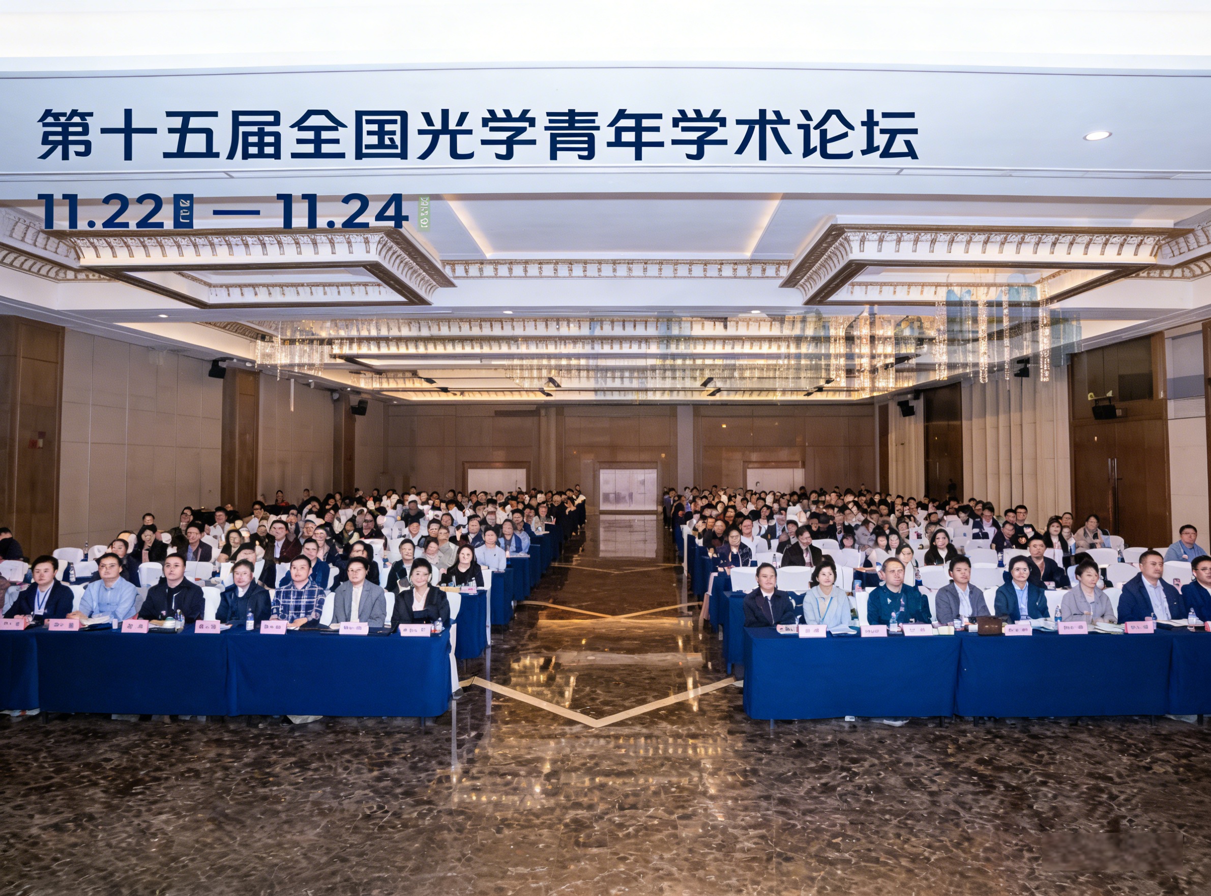
III. Concurrent Major Events
19 high-end academic summits, with leading keynote speeches by academicians and international experts, interpreting the cutting-edge trends of photonics technology.
The release event of new photoelectric productivity achievements and the exhibition of Golden Solder Award-winning products, focusing on breakthroughs in domestic high-end equipment.
The industrial chain leader forum, the university-enterprise research and development cooperation meeting, and the investment and financing roadshow will be held to open up channels for technology transfer and business cooperation.
The China Optoelectronics 100 Universities and 1000 Enterprises Talent Recruitment Fair and the Youth Optical Scholars Forum have been established to build a platform for talent exchange and cultivation.
IV. Core Highlights of the Exhibition
Authoritative Guidance:
Jointly organized by top domestic and international academic societies, with a powerful lineup of academicians and experts, it steers the technological trends of the industry.
Full-chain coverage:
One-stop display of achievements across the entire optoelectronic industry chain, from basic research, core components to terminal applications and equipment manufacturing.
Integration of production and research:
Deeply linking academic exchanges with industrial exhibitions to accelerate the market application of scientific research achievements and facilitate technological upgrades for enterprises.
Precise Matching:
Targeted invitations to professional purchasers, research institutes, and investment institutions to achieve efficient matching of supply and demand, technology, and capital.
International Perspective:
Gathering global optoelectronic enterprises and experts, building a cross-border exchange and cooperation platform, and promoting the export of domestic optoelectronic technology to the world.
V. Exhibition Viewing Guidelines
Admission method:
Free entry with pre-registration on the official website or WeChat official account. Identity verification by real name.
Target audience:
R&D, procurement and management personnel in the optoelectronics industry, scholars from universities and research institutes, investment institutions and industry practitioners.
Warm reminder:
During the exhibition, strictly abide by the epidemic prevention and safety regulations of the venue, and visit and negotiate in an orderly manner.
We sincerely invite colleagues from all walks of life to attend the grand event at the Beijing National Convention Center, to enjoy the feast of optics and photonics, explore new opportunities in the industry, and jointly build a new future for the development of the photonics industry!
Recent Articles